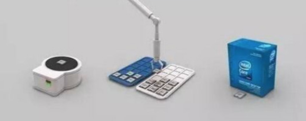
An integrated circuit is a microelectronic device or component. A process is used to interconnect the components, such as transistors, resistors, capacitors and inductors, etc. required in a circuit, to make them on a small chip or several small pieces of semiconductor wafers or dielectric substrates, and then encapsulate them in a shell to become a miniature structure with required circuit functions. All the components have formed a whole structure, which makes the electronic components step forward to miniaturization, low power consumption, intelligentization and high reliability. It is represented by the letter "IC" in the circuit. The inventors of integrated circuits are jack kilby (Ge based integrated circuit) and Robert noyce (Si based integrated circuit). Most applications in the semiconductor industry today are silicon based integrated circuits.
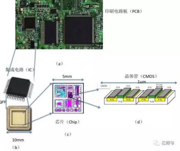
What exactly is an integrated circuit? Let's take the processor as an example and look at its manufacturing process.
Manufacturing process, in a nutshell, the processor can be roughly divided into sand material (quartz), silicon ingot, wafer, lithography (offset printing), etching, ion implantation, metal deposition, metal layer, interconnection, wafer and cutting, the core level of encapsulation, testing, packing list, and many other steps, and each step inside and contains more detailed process.
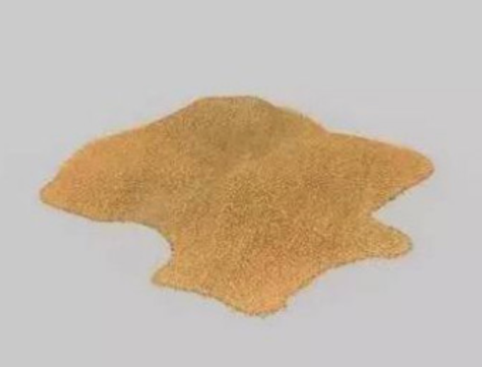
Sand: silicon is the second most abundant element in the earth's crust, and deoxygenated sand (especially quartz) contains up to 25% silicon in the form of SiO2, which is also the foundation of the semiconductor manufacturing industry.
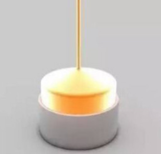
Silicon melting: 12 inch /300 mm wafer grade, same below. A silicon that can be used in semiconductor manufacturing quality, known as electronic grade silicon (EGS), is obtained by multiple purification steps. There is at most one impurity atom per million silicon atoms. This diagram shows how large crystals are obtained through the purification of silicon. The final product is the Ingot.
Monocrystalline silicon ingot: the whole is basically cylindrical, weighs about 100 kg, the purity of silicon is 99.9999%.
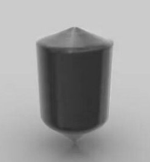
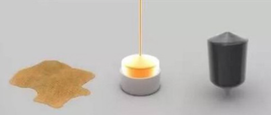
Silicon ingot cutting: a single sheet of silicon that is cut horizontally into a circle, also known as Wafer. By the way, do you know why the wafers are round?
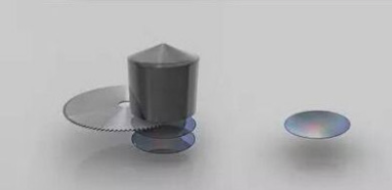
Wafer: the cut wafer is polished to almost flawless perfection, with a surface that can even be used as a mirror. In fact, Intel doesn't make the wafers itself, but instead buys the finished products directly from third-party semiconductor companies and USES its own production line for further processing, such as the 45nm HKMG(high-k metal grid) currently in the mainstream. It's worth noting that the original wafer Intel used was only 2 inches /50 millimeters.
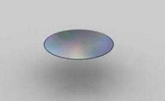
Photo Resist: the blue part of the image is a photoresist liquid applied to the wafer as it rotates, similar to the one used to make traditional film. The wafer rotation makes the photoresist very thin and very flat.
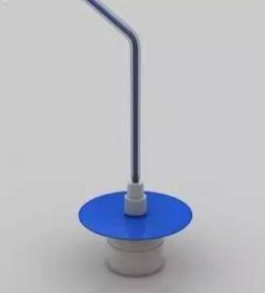
Photolithography: the photoresist layer is then exposed through a Mask under ultraviolet (UV) light and becomes soluble, during which a chemical reaction is similar to the change in film at the moment a mechanical camera shutter is pressed. A pre-designed circuit pattern is printed on the mask, through which ultraviolet light shines on the photoresist layer, forming each layer of the microprocessor. Generally speaking, the circuit pattern obtained on a wafer is a quarter of the pattern on the mask.
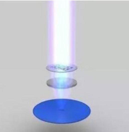
Photolithography: from this to the transistor level of 50-200 nanometer size. Hundreds of processors can be cut out of a single wafer, but from here you start narrowing your horizons to one of them, showing how to make components like transistors. The transistor ACTS as a switch, controlling the direction of the current. Today's transistors are so small that about 30 million can fit on a needle.
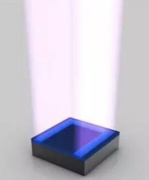
Dissolving photoresist: the photoresist exposed to ultraviolet light dissolves during lithography, leaving patterns consistent with those on the mask.
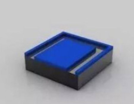
Etching: use chemicals to dissolve the exposed wafer, and the remaining photoresist protects the parts that should not be etched.
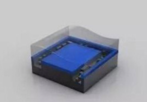
Clear photoresist: after the completion of the etching, the mission of photoresist is completed, and the circuit pattern can be seen after all clearance.
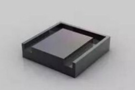
The fourth stage

Photoresist: reapply the photoresist (the blue part), then photolithography, and wash away the exposed part. The remaining photoresist is still used to protect the part of the material that will not be ion-injected.
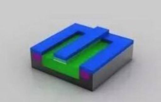
Ion Implantation: in a vacuum system, the solid material is irradiated (injected) with accelerated ions of doped atoms to form a special layer of Implantation in the areas to be injected and to change the electrical conductivity of the silicon in those areas. When accelerated by an electric field, an ion stream can travel at speeds of more than 300,000 kilometers per hour.
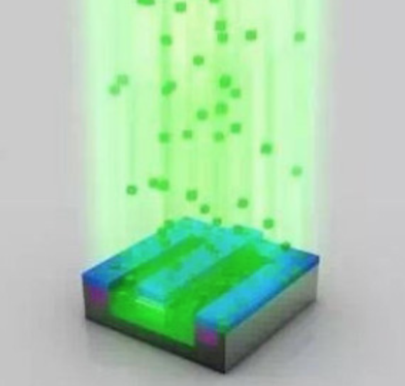
Clear photoresist: after ion implantation, the photoresist is also cleared, and the injection area (green) is doped with different atoms. Notice that the green is different now than it was before.
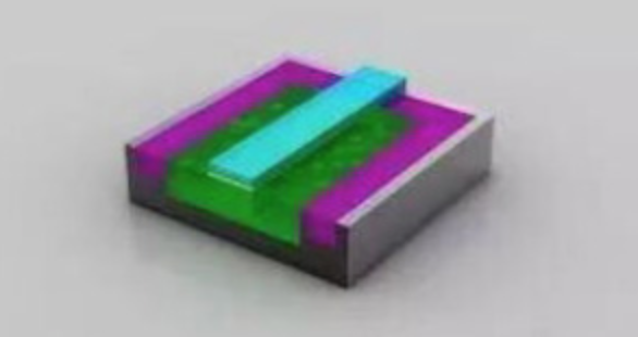
The fifth stage

Transistor ready: at this point, the transistor is almost complete. Three holes are etched into the insulation (magenta) and filled with copper to interconnect with other transistors.
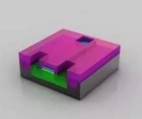
Electroplating: plating a layer of copper sulfate on a wafer to deposit copper ions onto a transistor. Copper ions go from the positive (anode) to the negative (cathode).
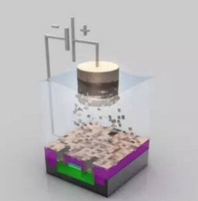
Copper layer: after electroplating, copper ions are deposited on the surface of the wafer to form a thin copper layer.
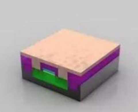
The sixth stage
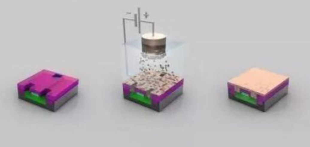
Polishing: to polish off excess copper, that is, to polish the surface of a wafer.
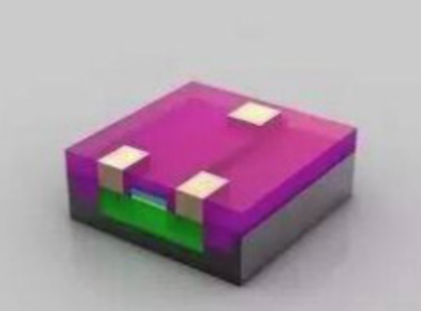
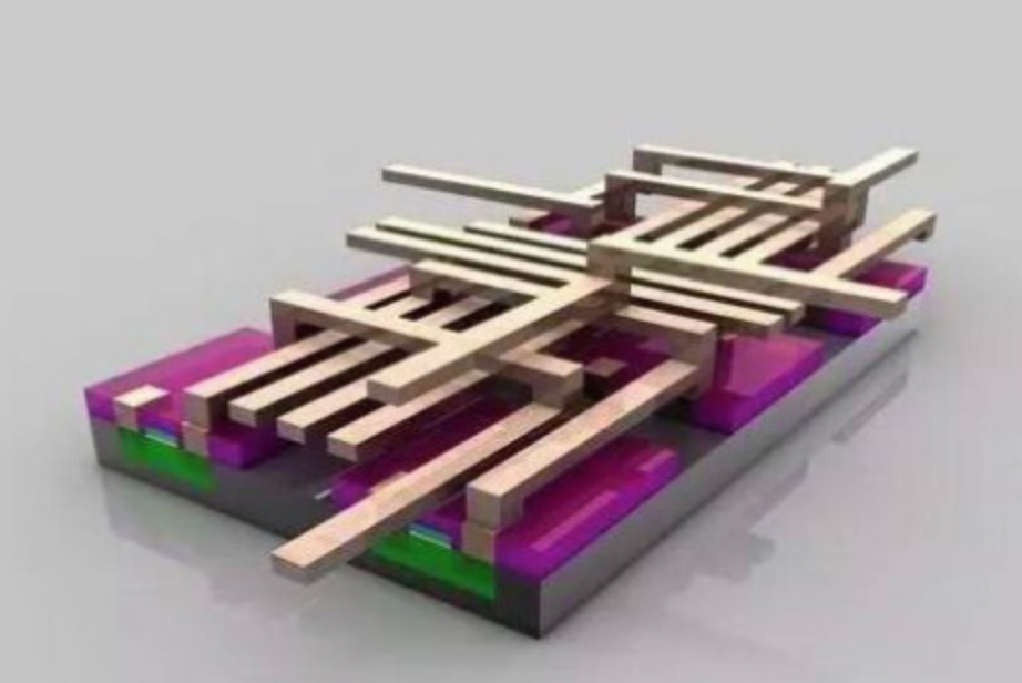
Metal layer: transistor level, a combination of six transistors, about 500 nanometers. A composite interconnect metal layer is formed between different transistors, and the specific layout depends on the different functions required by the corresponding processor. The chip's surface looks remarkably smooth, but in fact it may contain more than 20 layers of complex circuits, which can be magnified to reveal an extremely complex network of circuits shaped like a futuristic multi-level highway system.
The seventh stage
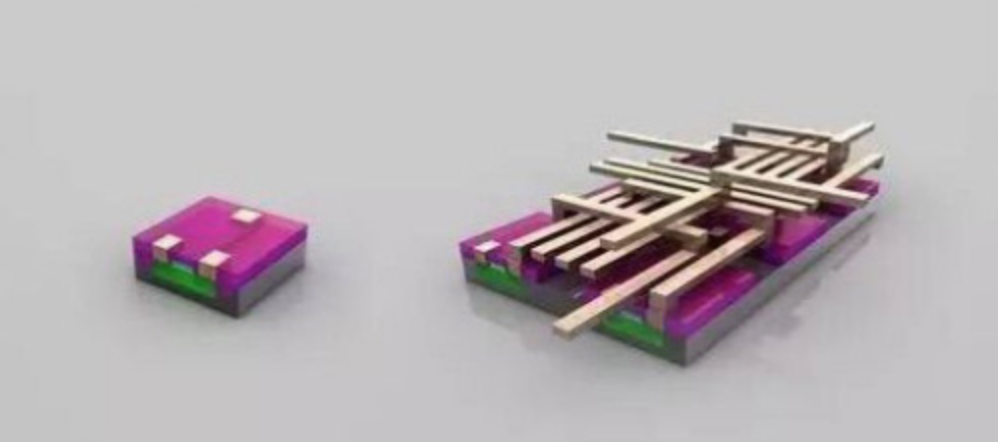
Wafer testing: kernel level, about 10mm / 0.5in. A portion of the wafer is pictured, undergoing the first functional test, using a reference circuit pattern to compare each chip.
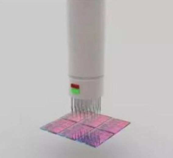
Slicing: wafer level, 300 mm /12 inches. The wafer is cut into chunks, each of which is a processor core (Die
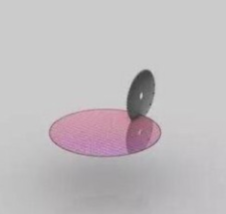
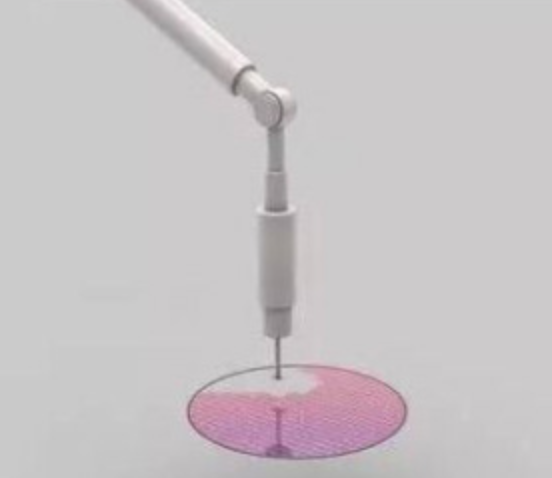
Defective core: wafer level. The faulty kernel found during the testing process was discarded, leaving intact preparations for the next step.
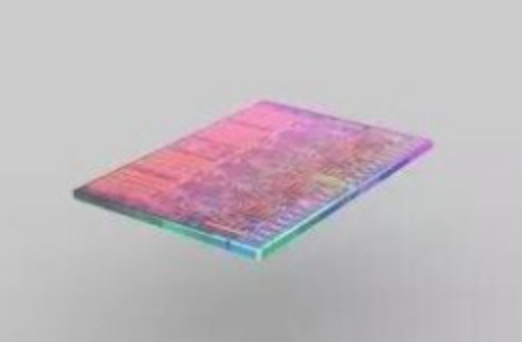
Single kernel: kernel level. A single Core cut from a wafer, shown here as Core i7.
Package: package level, 20 mm /1 inch. The substrate (substrate), the core, and the radiator are stacked together to form what the processor looks like. The substrate (green) ACTS as a base and provides an electrical and mechanical interface to the processor core to facilitate interaction with other parts of the PC system. The radiator (silver) is responsible for the core cooling.
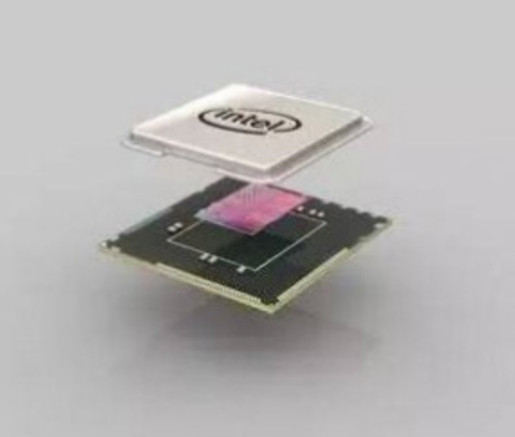
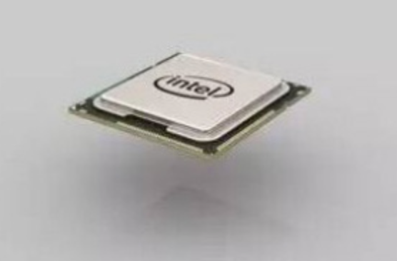
Processor: this gives you the full processor (here is a Core i7). The most complex product made in the cleanest room in the world actually comes through hundreds of steps, and here are just some of the key steps.
The ninth stage
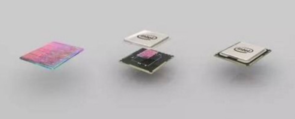
Rating test: the final test identifies the key features of each processor, such as the highest frequency, power consumption, heat output, etc., and determines the processor's rating, such as whether it is suitable for the top-end Core i7-975 Extreme or the low-end Core i7-920.
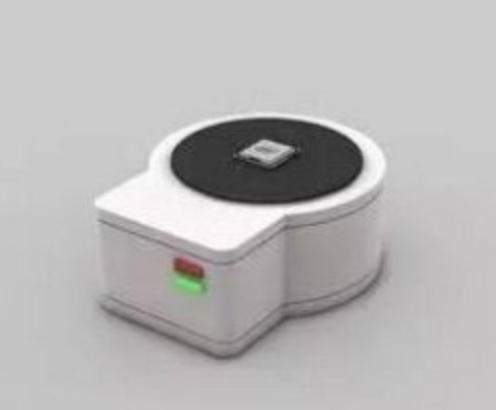
Boxing: load the same level of processors together based on the level test results.

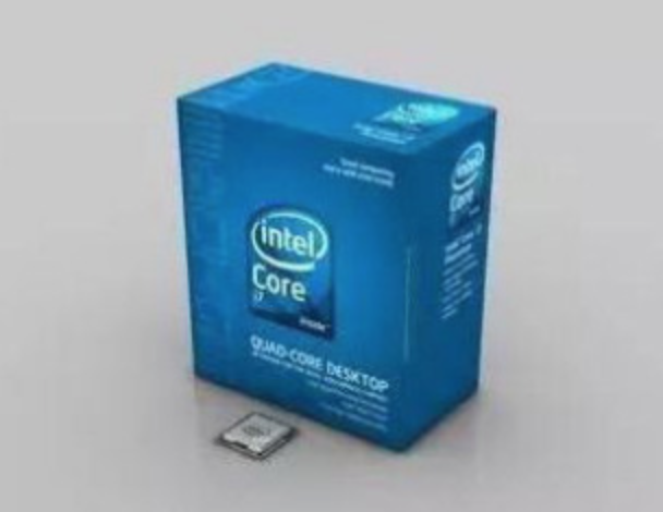
Retail packaging: manufactured and tested processors are either delivered in bulk to the OEM or are packed in boxes to enter the retail market. So let's take Core i7 again.
The tenth stage
