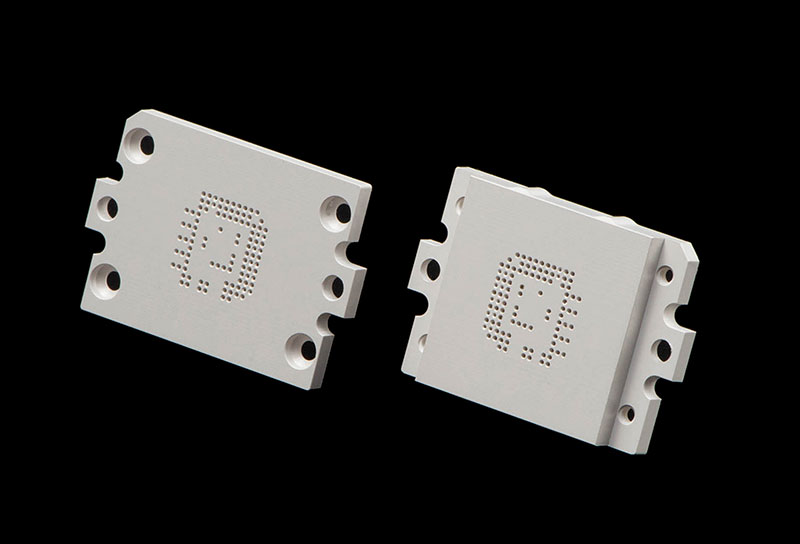
Test socket guide plates micromachining represents the pinnacle of high-tech precision in the semiconductor testing landscape. Harnessing advanced techniques, this application seamlessly navigates the intricate geometries of cutting-edge semiconductor architectures. In a world where nanometers make a difference, micromachining emerges as the avant-garde solution, ensuring flawless alignment and impeccable testing fidelity in an ever-evolving tech-driven world.
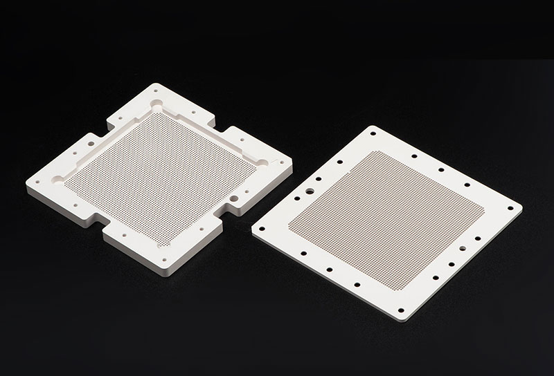
Test socket guide plates micro-machining results and achievements
Product Size:0.7x82x82mm, deformation ± 0.01mm, no burrs after enlarging the micropores by 100 times.
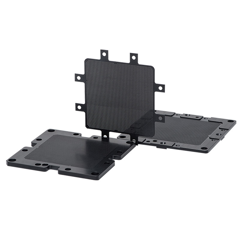
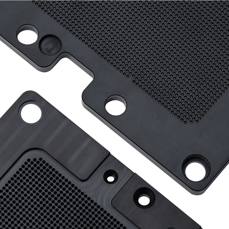

We have 20 years of experience in engineering plastic processing, no matter what problem you encounter? For example: extremely difficult to control deformation, concentricity, position, etc., especially test sockets.
Round holes of Ø 300 μm are milled with a 350 μm pitch into both Torlon and Vespel materials, featuring a 500 μm thickness and an impressively swift cycle time of 0.6 seconds. Torlon also accommodates a countersunk step hole, precisely measured at Ø 3.0 mm with a 1 mm depth and Ø 2.5 mm with a 0.8 mm depth. In contrast, Vespel showcases the expertise with step holes from Ø 400 μm down to 650 μm, set at a pitch of 750 μm, and through holes meticulously drilled to Ø 200 μm and a depth of 650 μm.
You currently have a test socket guide plate micromachining project and you would like to know what we could achieve together?
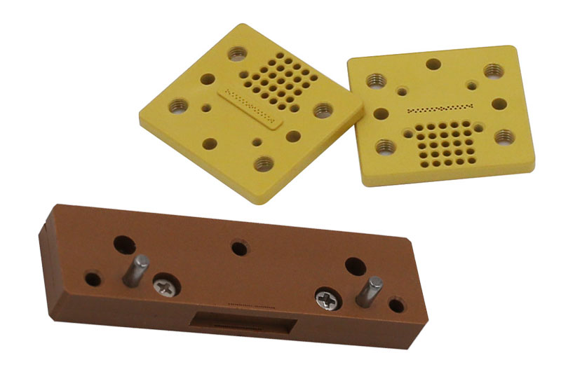
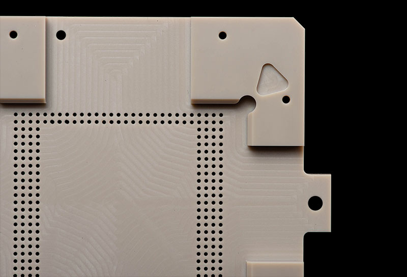
Machining plastic is just one of our specialties in plastic machining. We have solutions for all aspects of plastic machining. If you have any questions about CNC machining at Novaplas Precision, please don't hesitate to contact us. The contact details can be found below.